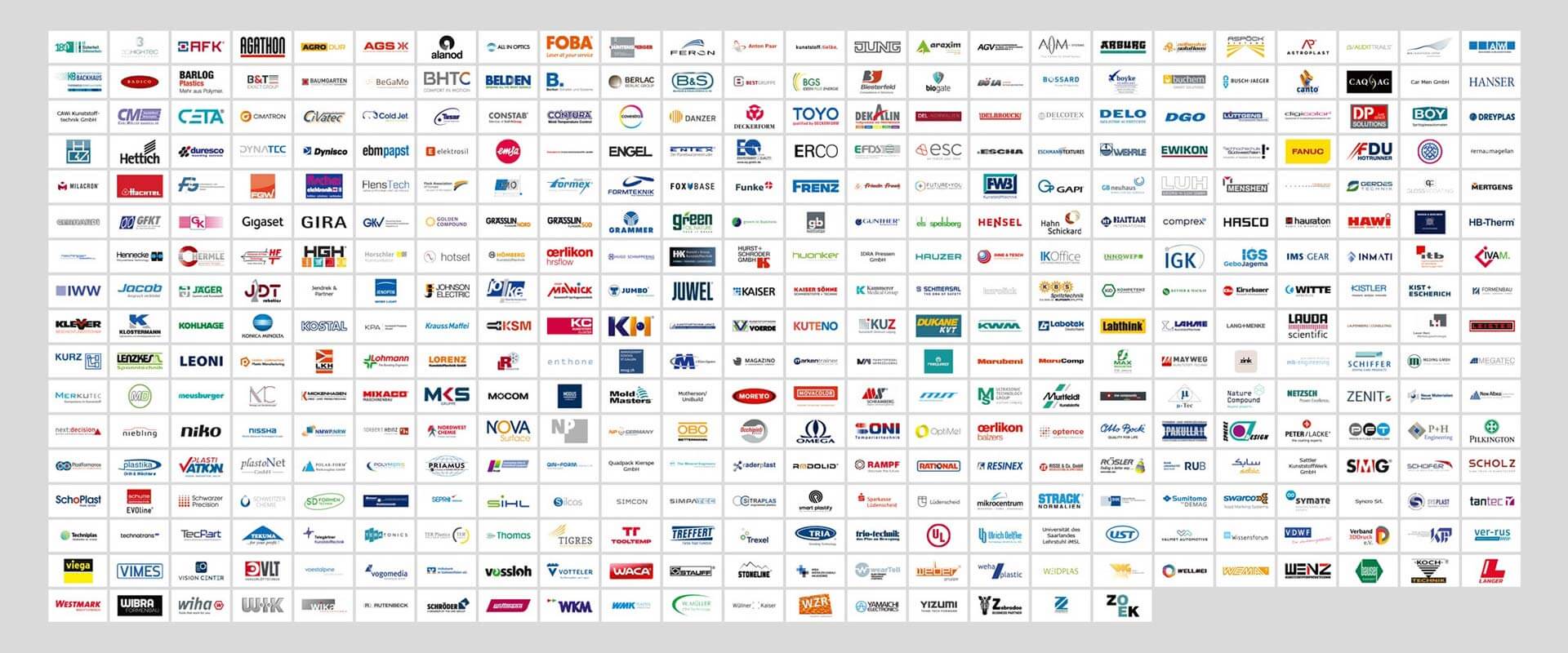
The Kunststoff-Institut Lüdenscheid is a unique network with access to over 400 partners along the value chain in the plastics industry.
Holistic companion
With our holistic KIMW 360° approach, we think and act across disciplines. Our interdisciplinary teams combine technical expertise, scientific depth, and industrial practice to develop customized solutions together with you.
Learn more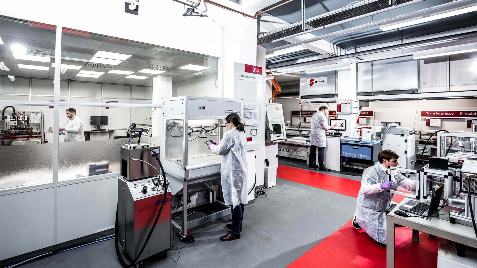
Transfer partners
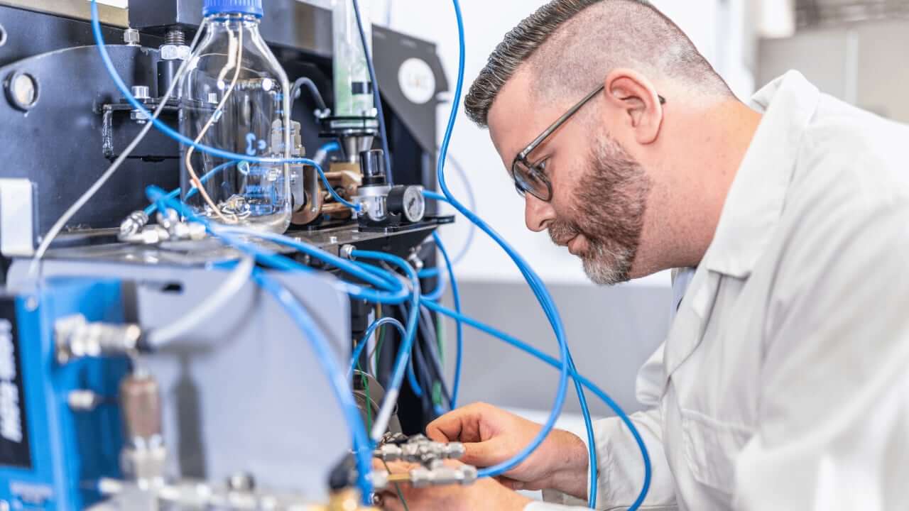
We are a technical caretaker and service provider for process and tool technology inquiries. Under services you will find everything about material selection and development, application technology, surface coating, testing as well as sustainability and management topics.
Get in touch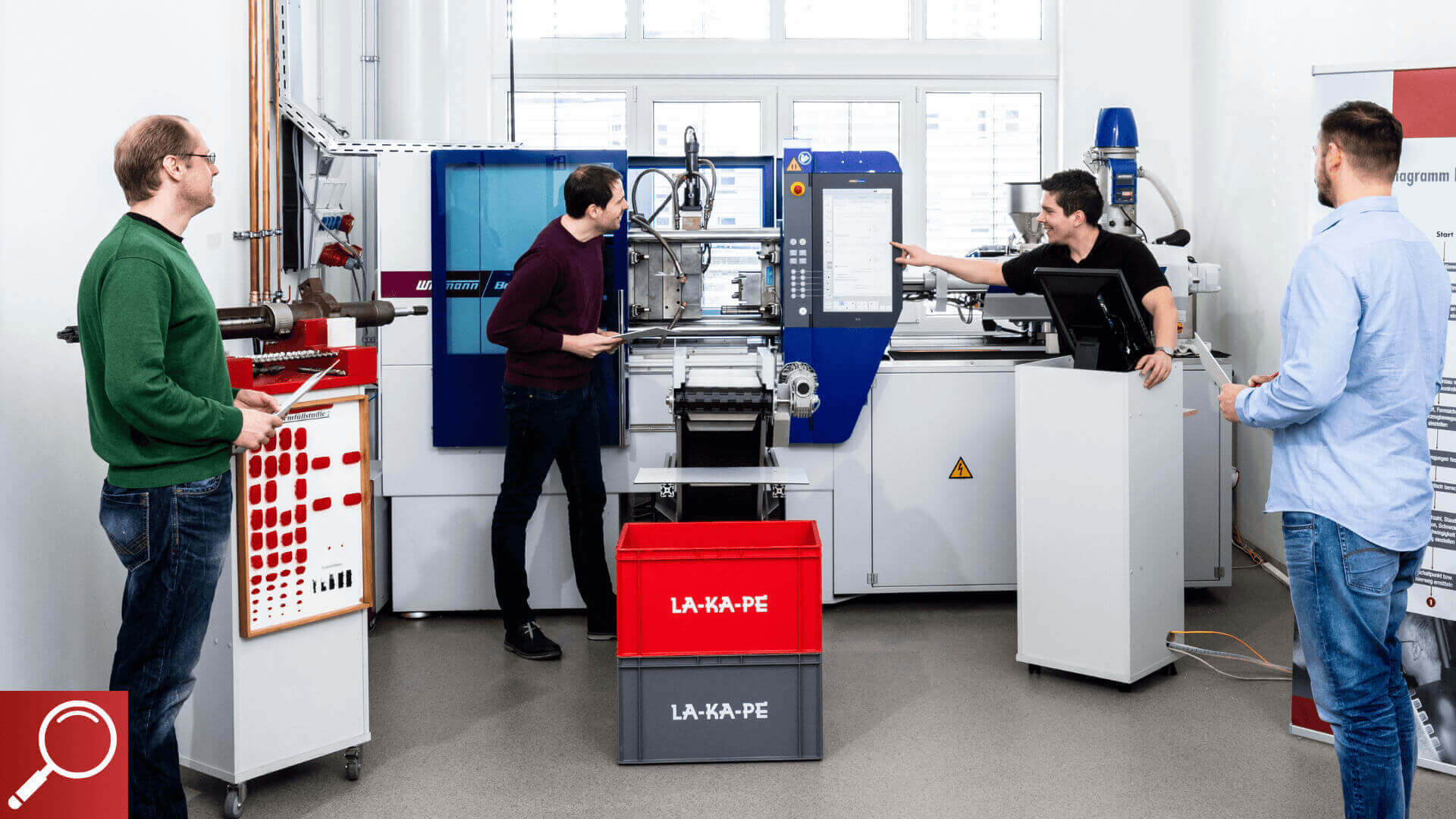
Innovation drivers
We are application-oriented researchers and developers who focus on new innovations, products and processes and involve you as a corporate partner. You can find everything you need to know about innovation under Research.
Learn more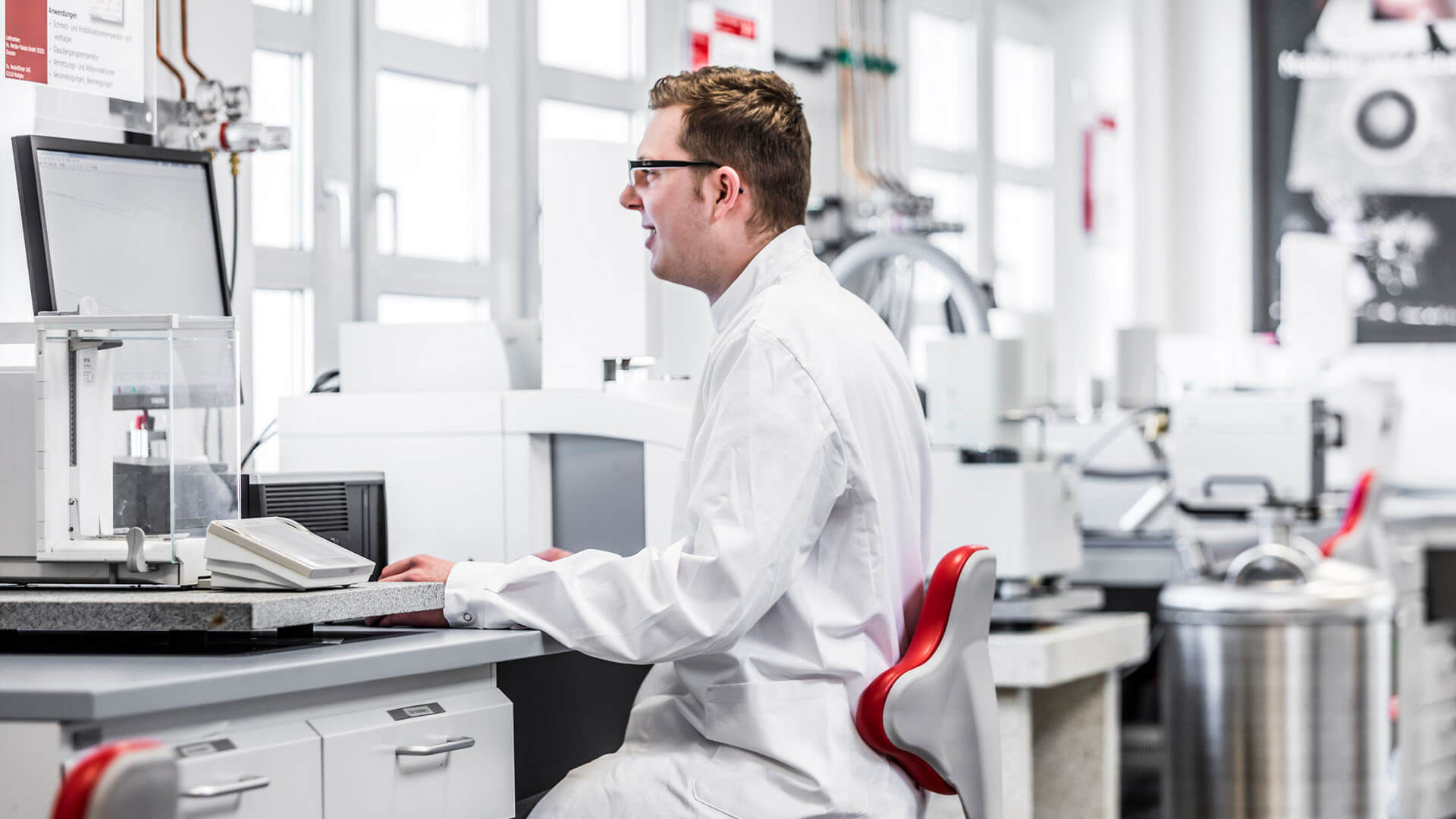
What we do
As a customer of the Kunststoff-Institut Lüdenscheid, you benefit from a comprehensive range of services covering all aspects of plastics.
We see ourselves as a neutral, practical and technology-oriented point of contact for all issues along the entire value chain – across all industries. From the initial idea to the production-ready component, we support companies on their way to the optimum solution.
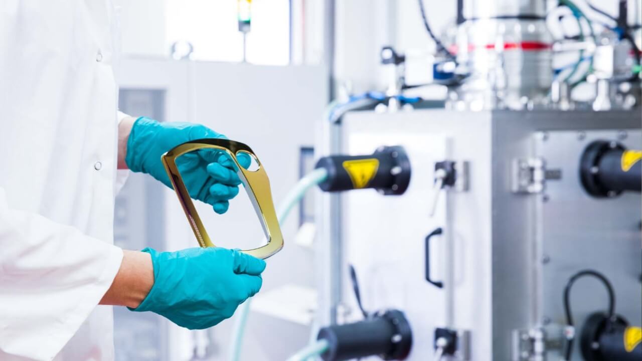
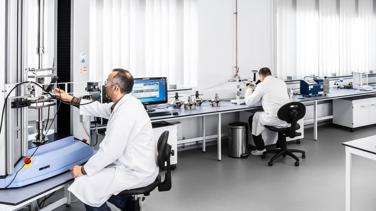
Our institute not only offers in-depth expertise and many years of experience, but also modern laboratories, testing facilities and pilot plants that enable the development, testing and optimization of products and processes at the highest level. We don’t just look at individual issues, but think holistically – from material selection and tool technology to the finished application.
Whether you are a small business or a large corporation – we provide you with individual support for your technical challenges, provide impetus for innovation and sustainability or connect you with suitable partners from our broad network of experts.
Together with you, we develop solutions that work in practice and give you the decisive edge.
A powerful network
The portal for the plastics industry
Events
-
04.+05.02.2026
Spritzgießen Thermoplaste – die Basics
Lüdenscheid Seminar -
10.02.2026
ECO.MATERIALScon
Lüdenscheid, Online Fachtagungen/Fokustage/Foren -
10.+11.02.2026
Formteilfehler an thermoplastischen Spritzgussteilen
Lüdenscheid Seminar -
11.02.2026
Lesen von Simulationsergebnissen
Lüdenscheid Seminar -
09.-12.02.2026
Ausbildungsprogramm Ingenieurnahe Qualifikation: Produktentwicklung
Lüdenscheid Weiterbildung -
12.02.2026
Formteilfehler – Werkzeug oder Produktion?
Lüdenscheid Seminar -
17.+18.02.2026
Workshop Prüfungsvorbereitung Verfahrensmechaniker
Lüdenscheid Seminar -
17.-19.02.2026
Einstieg in die Spritzgießtechnik
Lüdenscheid Seminar -
19.02.2026
Werkzeugtechnik für Kaufleute
Lüdenscheid Seminar -
ab dem 23.02.2026
Verfahrensmanager Spritzgießtechnik (IHK)
Lüdenscheid Lehrgang

